

The CHIPS and Science Act of 2022 made historic investments in semiconductor research, workforce development and manufacturing. Below, and in the sidebar links, learn about how UW ECE is leveraging these opportunities.
UW ECE and the CHIPS and Science Act
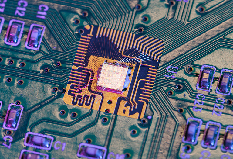
A recently designed microchip from the lab of UW ECE Professor Chris Rudell (in gold, mounted to the green circuit board shown above). This chip is a 2.4 GHz full-duplex transceiver, which employs multiple self-interference cancellation techniques to improve signal fidelity and efficiently use limited bandwidth. The chip has a broad range of applications, including use in satellite communications and radar, shipping, aviation and space industries, and 5G technologies. Photo by Ryan Hoover / UW ECE
UPWARDS for the Future
The University of Washington is at the forefront of an international effort to innovate the semiconductor industry while building a skilled U.S.-based workforce to design and manufacture chip technology. UW ECE and Physics Professor Mo Li is leading the University’s contribution to this effort. More>>
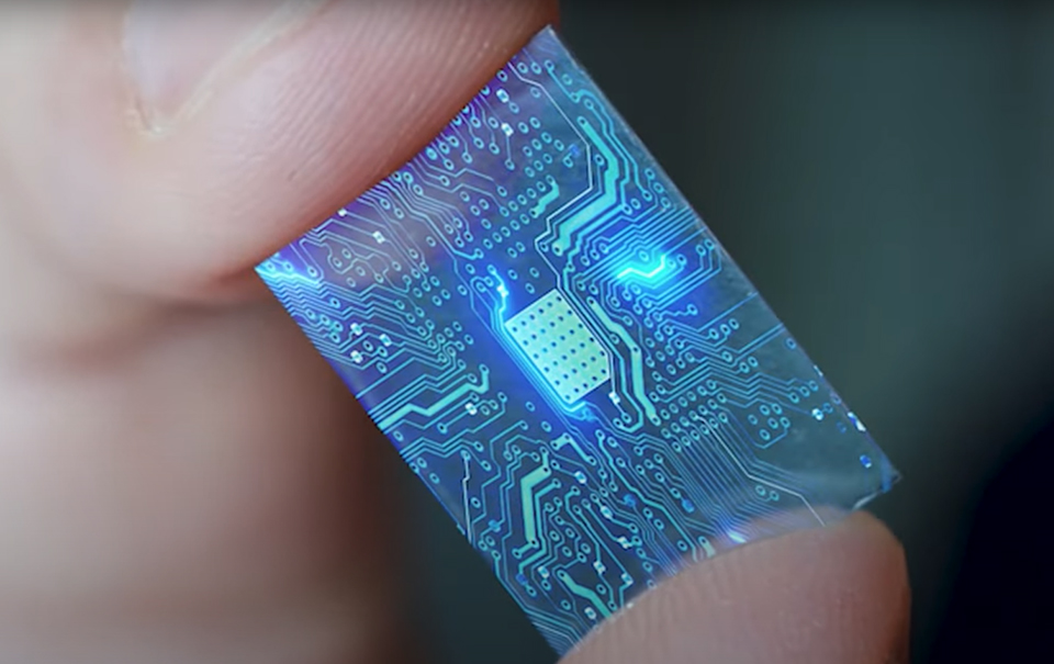
UPWARDS for the Future will support work already underway in the UW’s Washington Nanofabrication Faciliity. The photo above is from a video by Kiyomi Taguchi / UW News.
Joshua Collier and Jakob Stickles, undergraduate students in the UW’s Pathways for Inclusive Excellence program, show off the silicon wafer that they produced during a Washington Nanofabrication Facility workshop. They successfully built and tested diodes, resistors, and capacitors. Photo provided by the Washington Nanofabrication Facility.
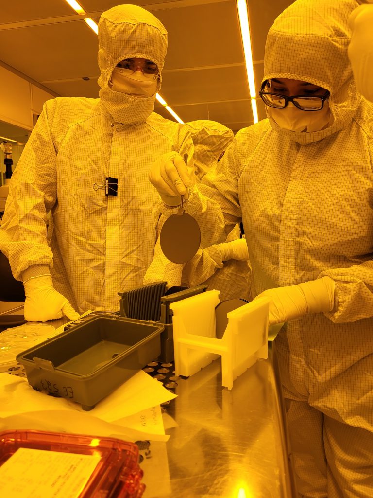
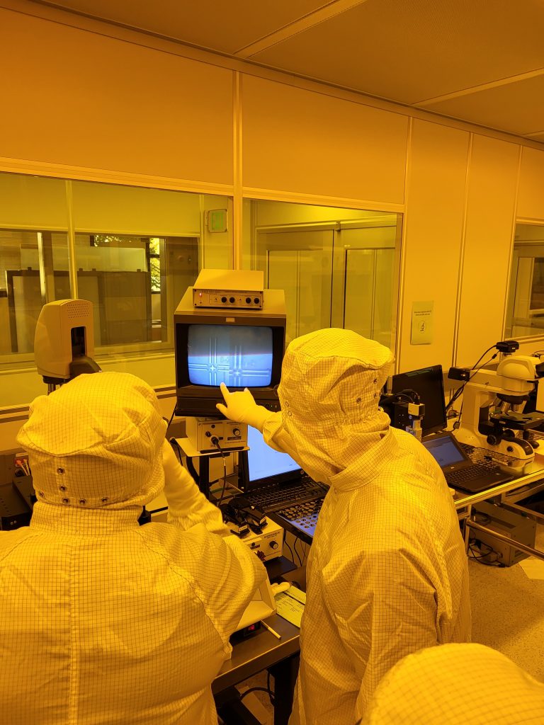
Washington Nanofabrication Facility course instructor Darick Baker teaches Megan Castellanos and Joshua Huber how to pattern their wafer during the Nanofabrication workshop. Castellanos and Huber are undergraduate students in the UW’s Pathways for Inclusive Excellence program. The students worked together to build wafers with semiconductor devices in the Washington Nanofabrication Facility. Photo provided by the Washington Nanofabrication Facility.