

Story by Wayne Gillam | UW ECE News
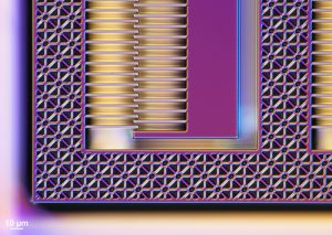
Polarized light microscopy captured this colorful image of an electrostatic comb drive contained within the lens developed by the UW ECE research team. One thing that makes the team’s lens unique is that it uses metasurfaces — thin, fabricated plates that transmit and diffract light — activated and operated, or “actuated,” by this microelectromechanical system, or MEMS.
Most of us use the cameras in our cellphones and laptop computers every day. However, many people don’t realize that miniature lenses are crucial for these devices to operate. As the size of digital electronics and other technologies continues to shrink, the demand for smaller, more efficient optical components is growing. Small cameras are useful tools for many applications, such as robotics and surveillance, aerospace, and biomedical systems. Most tiny cameras, as well as the devices they inhabit, would benefit from even smaller, more reliable and cost-effective lenses, but crafting lenses that are smaller than what exists in the market today is a challenge for engineers.
To be useful in most applications, a camera lens needs to be tunable — it must have the ability to focus and be able to zoom in and out on an image. However, most optical systems in current use are made up of relatively bulky elements that can be challenging to produce, or they use tuning mechanisms that require a large volume of space to work. Researchers have been tackling these problems for a while now, but the lenses that have been produced so far often have issues with respect to power consumption, tuning speed, fabrication cost and production scalability.

The UW ECE research team, from left to right: graduate student Zheyi Han, recent graduate Shane Colburn, associate professor Arka Majumdar and professor Karl Böhringer
In a recent paper published in Nature Microsystems & Nanoengineering, a UW ECE research team describes a new type of micro-optical device that successfully addresses these challenges. The team was led by professor Karl Böhringer, director of the Institute for Nano-Engineered Systems, and associate professor Arka Majumdar, who is also an associate professor in the UW Department of Physics, as well as a member of NanoES and the Molecular Engineering & Sciences Institute. The research was funded by Böhringer and Majumdar’s startup, Tunoptix, and the team fabricated their lens prototype in the Washington Nanofabrication Facility, which is supported by the National Nanotechnology Coordinated Infrastructure through the National Science Foundation.
“We’ve built optical components that are small and compact, as well as fast and relatively easy to produce in mass fabrication processes,” Böhringer said. “Specifically, we’ve created a tunable lens, but the tuning is not happening in the conventional way that might come to mind, like what exists in a telescope or microscope.”
How the lens works
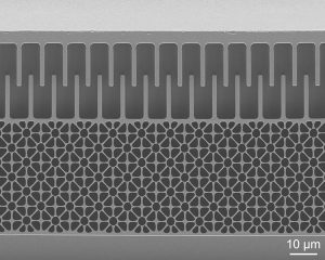
Scanning electron microscope image of the MEMS-actuated platform carrying one of the two metasurface plates used in the lens. The metasurface plate shown is the square object at the center of the lens, flanked by the electrostatic comb drive on either side. The other metasurface plate is on a stationary substrate (not shown), which is overlaid on top of this platform.
In traditional optical systems, like what you might find in a telescope, microscope or binoculars, lenses are made out of clear glass or plastic elements and move closer to or further away from each other in order to focus or zoom in and out on an object. But the UW ECE team’s prototype works in an entirely different way. Instead of being glass or plastic, their lens is made out of silicon nitride, and it is shaped into thousands of comb-like nanostructures that flank two square plates coated with millions of microscopic 3D posts, called nanopillars. The square plates are considered “metasurfaces” because they are made out of an artificial sheet material constructed with sub-wavelength patterns. The plates transmit and diffract light, and they were fabricated in a unique process Majumdar developed in his lab.
“These metasurfaces have an interesting property, in that if you design them properly, they can focus light,” Böhringer explained. “If you take these surfaces, place them in close proximity and move them relative to each other, you can actually create a lens with a tunable focal length.”
The metasurfaces are extremely thin, almost two-dimensional, making the optical device only about two microns thick. For comparison, that is much thinner than the width of a human hair, which is approximately 70 microns thick. It is also thinner than the wavelength of infrared light, which the team used in their optics research. With metasurfaces, complex and bulky geometric lens curvatures can be converted into a space-saving, flat surface with a thickness measured in nanometers. And although this lens might seem difficult to build because it is intricate, complex and microscopic, the fabrication process uses already-existing semiconductor nanofabrication technologies. This means that the team’s lens can be scaled-up for low-cost, mass production.
“This is a very different way of thinking about optics,” Majumdar said. “Each of the metasurfaces are not lenses on their own. They are completely different kinds of structures. But when you put them together and laterally displace them a little bit, you get a lens-like behavior.”
MEMS meets metasurface optics
Scanning electron microscope image of the comb-like nanostructures that make up the electrostatic comb drive, which is part of the lens’ microelectromechanical system, or MEMS.
This type of optical lens is called an “Alvarez lens” because the physical principle it operates on was discovered by Luis Alvarez in the 1960s. What makes this Alvarez lens unique is that it uses metasurfaces that are activated and operated, or “actuated,” by a microelectromechanical system, or MEMS.
“Our device is driven electrostatically. You’re applying a voltage, and the electrostatic field that you get between two different electrodes pulls the structures that make up the metasurfaces in a particular direction,” Böhringer explained. “If you use electrostatic actuation, it basically means there is no direct current flowing after the initial charge, and the power consumption is very low.”
MEMS-actuation makes the lens capable of producing a change in focal length that is ten times larger than the actuated displacement of the plates that make up the metasurfaces. This translates to a wider tuning range than many of the comparable lenses on the market today. It is also very fast, with tuning speeds typically running under a millisecond. That is orders of magnitude faster than liquid tunable lenses, which are currently the industry standard and operate on a principle similar to the lenses in our eyes.
“That’s really a major advantage compared to these liquid lenses, which have some inertia and some viscosity. They are much slower than these tiny structures that we built,” Majumdar said. “Another problem with liquid lenses is temperature instability. When you heat up a liquid, it expands more than a solid. A MEMS-actuated lens doesn’t have this temperature fluctuation problem as compared to liquid lenses.”
The research team asserts that combining flat, super-thin metasurfaces together with the MEMS-driven Alvarez structure will allow for the ultimate miniaturization of optical devices with a tunable focal length, making their lens more mechanically and thermally robust than other engineering approaches, with key advantages such as fast tuning, compact size, light weight and low energy consumption.
What the future holds
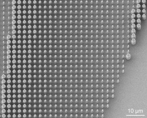
Scanning electron microscope image of the 3D nanopillars that cover the two metasurface plates that reside in the middle of the lens. The metasurfaces transmit and diffract light, and they were fabricated in a unique process Majumdar developed in his lab.
This research was conducted using infrared light. Next steps for the research team will be to scale-down the size of the nanopillars on the lens’ metasurfaces even further, in order to work with visible light, which has a shorter wavelength than infrared. This will increase the number of potential real-world applications for the technology.
The team also wants to explore operating each of the nanopillars that reside on the lens’ metasurfaces independently.
“These metasurfaces contain millions of light-scatterers, small, 3D nanopillars,” Majumdar said. “Currently, we are changing all of them at the same time, not moving them independently. But if you could start changing each of the elements separately, it would definitely change the way people think about optics and what is possible.”
If the team were able to accomplish this next step, it would open up an entirely new line of research and new applications for the technology.
“If this next step works, if we can really change millions of degrees of freedom in the lens’ nanopillars, then I can envision applications in deep tissue imaging,” Majumdar said. “You wouldn’t need to do X-ray imaging or MRIs in the traditional way. You could see everything inside your body with a cell phone camera. That’s the type of thing it would enable.”
Operating each nanopillar independently would enable the lens to see through highly diffuse and dense materials (such as your body) in a manner somewhat similar to how a vehicle’s fog lights help to illuminate a cloudy night.
“It’s also good to point out that there would be nothing outrageously expensive about that. It’s not a device that in the end would cost millions of dollars,” Böhringer added. “Of course, there is still a lot of research to be done to get something like that to work, but eventually, I think this could be something that’s in every household or maybe in every phone.”
The ways in which the team’s MEMS-actuated metasurface Alvarez lens could evolve are admittedly a bit uncertain for now, but one thing is for sure — the lens this team has developed is desirable for a wide range of imaging and display applications today. In the future, it could help us see the world through tiny cameras like never before.