

When it comes to lenses, we expect a lot: perfect zooming capability on our camera phones, a flawless 3D visualization experience with augmented reality glasses, and compact and simplified variations of microscopes. Traditional glass lenses have limitations on how much they can do. Metasurface optics—which are ultra-thin, manufactured, man-made surfaces—are advancing the world of optics.
In a paper published in July in Optica, researchers in the Department of Electrical Engineering and Physics at the University of Washington announced that they created a thin optical component to transcend the capability of a regular lens.
“This lens is very thin, close to one micron, which has the thickness of 1/100th of a strand of hair,” said senior author Arka Majumdar, assistant professor of electrical engineering and physics. “We wanted to make a very small optical component to create more advanced, tunable flat optics.”
Their design consisted of two metasurfaces, which are nano-patterned films of material that can very abruptly change properties of light. The two metasurfaces work together to form what is called an Alvarez lens, a lens that has a focal length that can be changed by moving the two metasurfaces past one another sideways. To build their device, they used similar fabrication techniques compared to what are used to make the electronic chips found in phones and computers.
The researchers also developed fabrication techniques to build large-area metalenses, with hundred’s of millions nano-scale scatterers. To fabricate such a massive number of scatterers, they developed a compression algorithm to generate the pattern used for fabricating the devices. Using the fabricated Alvarez metalens, Majumdar and his team reported the largest tunable focal length range for an optical metasurface demonstrated to date. They also demonstrated zoom imaging at visible frequencies with a metasurface for the first time. Previously they reported full-color imaging at visible wavelengths using computational imaging along with a new type of metalens.
“We plan to now bring those computational techniques together with our large area fabrication and tunable lenses to create optical systems, with potential applications in mixed reality systems,” said Majumdar.
There is already strong interest from various companies in similar research and this specific work was funded by Samsung and Amazon.
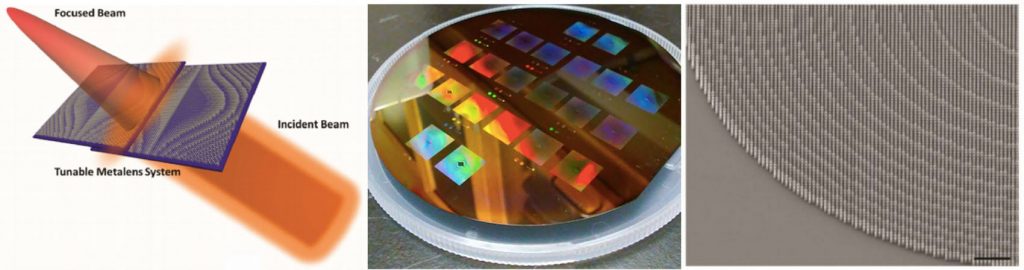
The two cubic metasurfaces can be laterally displaced to create a tunable focal lens. The metasurfaces are large with millions of nano-scatterers.