

UW ECE Assistant Professor Arka Majumdar and his team of researchers have solved a major problem in integrated optical information processing and communication using new phase-change materials.
Moving Beyond Moore
Over the course of the past few decades, perhaps nothing has transformed our daily lives more than the continued miniaturization of electronic integrated circuits. While computers were once room-sized, multi-million dollar luxuries housed in government research institutions, universities and large corporations like IBM, we now carry supercomputers in our back pockets that are several orders of magnitude more powerful than those onboard the space shuttle, and for just a few hundred dollars. The Internet has, no doubt, also played an increasingly important role in bringing computing to nearly every sphere of our lives since around the mid-90s.
Computer scientist and businessman Gordon Moore. photo: Science History Institute; commons.wikimedia.org/
Unfortunately, the technological pattern of scaling which has mostly held true in guiding this meteoric rise of computing until now, known as “Moore’s law”, is quickly coming up against another set of laws — those of physics, leading to its apparent end. Moore’s law was coined in 1965, named after Intel co-founder Gordon Moore’s astute observation that the number of transistors that fit onto an integrated circuit was able to double approximately every 18 months to two years, leading to exponential growth in computing power as a result.
It is not yet clear which “next big thing” in computing will emerge as the new dominant semiconductor material for transistors to continue this doubling trend into the foreseeable future. New, “exotic” materials with outstanding semiconducting properties such as graphene and carbon nanotubes have been proposed, but are still in the experimental phase and would require massive amounts of time and money to reconfigure fabrication facilities and processes to make them commercially viable.
Photonic information processing, however, which sends information using optical wavelengths in the visible or near infrared spectrums of light within photonic integrated circuits (PICs), is a new and very promising approach being considered as a solution to the “More-than-Moore” strategy. Because of their low latency (the delay in computing before a transfer of data begins following an instruction for its transfer), low energy loss, parallel computing capability and high speed, PICs have all of the desired qualities to carry computing into the next generation and beyond, with applications in neuromorphic computing, quantum information and microwave photonics. And thanks to existing fabrication technologies that are readily available and already highly sophisticated, it is now possible to manufacture such PICs at a large scale using silicon, the primary element that has been used to create transistors right from the start.
However, one important unsolved issue with this particular process has remained — how to create a switch that can reconfigure the PIC. Such reconfiguration allows programming of the same fabricated PIC to be used for a variety of different applications. An example of such a reconfigurable electronic circuit is a field-programmable gate array (FPGA), an incredibly versatile component that can be programmed to create any arbitrary circuit needed. However, the lack of compact, low-power optical switching elements thus far has prevented such functionalities in optics.
Pinning it down
A team at the University of Washington Department of Electrical & Computer Engineering (UW ECE) led by Assistant Professor Arka Majumdar, in collaboration with Intel, Stanford University, Ningbo University, and UW ECE Professor Scott Dunham and Associate Professor Mo Li, has solved this problem. Their paper, recently published in the scientific journal Advanced Materials, successfully demonstrates their ultra-compact, ultra-low power, non-volatile optical switch. Non-volatile memory has the ability to retain its stored data even if its power supply has been shut off, similar to a standard hard disk drive (HDD).
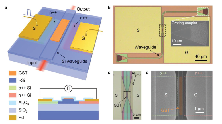
Figure 1. Nonvolatile electrically reconfigurable photonic switching units. a) Schematic of the device. For clarity, the top thin-film Al2O3 encapsulating layer is not displayed. Inset: cross-section of the device. b) Top-view optical microscope image of the switching unit on a waveguide with 10-nm-thick GST and a 5-µm-long active region. Inset: SEM image of the grating coupler. c) Optical microscope image of the black dashed area in (b). d) SEM image of the active region boxed in (c). False color is used to highlight the GST (orange). S (G), signal (ground) electrode. p++ (n++), heavily doped p (n)-type silicon region. i, intrinsic silicon region.
The key to this technology is a new kind of material which changes its phase from ordered (crystalline) to disordered (amorphous) states under electrical Joule heating. Using such phase-change materials, or PCMs, which either release or absorb energy during their phase transitions to provide heating or cooling, has previously been explored in the context of electronic memory (computer random access memory [RAM], for example). While several other groups have successfully demonstrated the reconfiguration of photonic devices using PCMs, all of these groups had used an external light beam as a source to actuate the switching mechanism. For large-scale systems with thousands of optical devices, though, it’s necessary to actuate such switching electronically.
This is precisely what the UW ECE team was able to accomplish by using a PIN diode-based heater in silicon. PIN diodes are wide regions of a semiconductor commonly used as RF switches, attenuators, photodetectors and phase shifters to convert alternating current to direct current (AC to DC), detect radio signals and emit or detect light.

PIN diode illustration by Georg Wiora, Wikipedia.
“We knew that the traditional heating used in electronic memory would not work for us, as the volume of the phase-change material that changes is miniscule,” said the lead co-author and UW ECE Ph.D. Research Assistant Jiajiu Zheng. “We needed an external heater, but the traditional metallic heaters also introduced a high amount of optical loss as metal absorbs the light and the energy is lost as heat.”
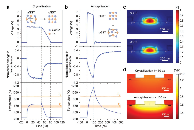
Real-time optical transmission during Set and Reset processes. a,b) real-time power of the applied electrical pulse (dashed line) and corresponding normalized change in optical transmission of the simulated switching unit at 1,550 nm (solid line) for crystallization (Set, a) and amorphization (Reset, b). Here, the length of the switching unit is 5 mm and the thickness of the GST is 10 nm.
That’s where the team came up with the idea of using a silicon-based heater. Silicon-based heaters are already being explored for applications that integrate photonic LiDAR, a method for measuring distances by illuminating the target with laser light and measuring the reflection with a sensor, and the UW ECE team used that same method to actuate the phase transition in their experiments. “But just having that idea was not quite enough,” said Majumdar. “We started doing this almost two years ago, but there were many material processing steps we had to figure out, including how to encapsulate the materials and what the ideal switching conditions are.” After much experimentation and simulation, however, the team finally figured out a process for the electrical switching to work as they had hoped.
Smaller, faster, ‘light’er
This new process has huge ramifications for the continued miniaturization of electronic components that are used in a variety of industries. “This is an extremely important step forward,” added Majumdar. “We are seeing novel phase-shifters that are able to be 1,000 times smaller than before, with zero static energy, and we can control all of this using an electronic signal.”
“This is an extremely important step forward.”
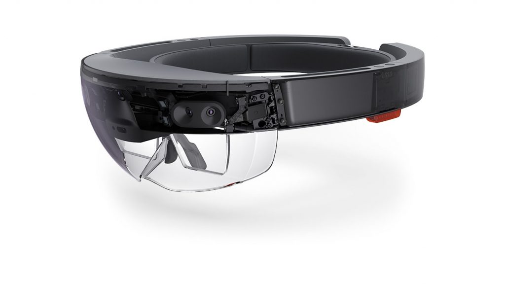
Microsoft Hololens augmented reality visor. photo: Wikipedia
With this invention, Majumdar is now creating large-scale, extremely low-power reconfigurable photonics that consist of over a thousand individual devices. These could have applications in consumer electronics such as optical FPGA, driverless car technologies and augmented reality visors like Microsoft’s Hololens, for example. When compared to currently available components, these optical switches can effectively steer light using just a fraction of the amount of power, and do so a thousand times faster, all without any moving parts.
The UW ECE team has already been approached by Boeing and NASA about their research, and the opportunities for using this reconfigurable photonic platform is, for the moment, seemingly endless.
Story by Arka Majumdar and Ryan Hoover | UW ECE News