

Interview by Renske Dyedov, originally published on Washington Nanofabrication Facility’s User Spotlight feature section.
University of Washington Electrical & Computer Engineering (UW ECE) Ph.D. candidate Zheyi Han has been a part of the Washington Nanofabrication Facility (WNF) community as both a student worker and as a graduate research assistant for over five years. In this Q&A, she tells us about her research integrating micro-electromechanical systems into compact optical systems and her hopes of joining an industrial research lab after graduation.
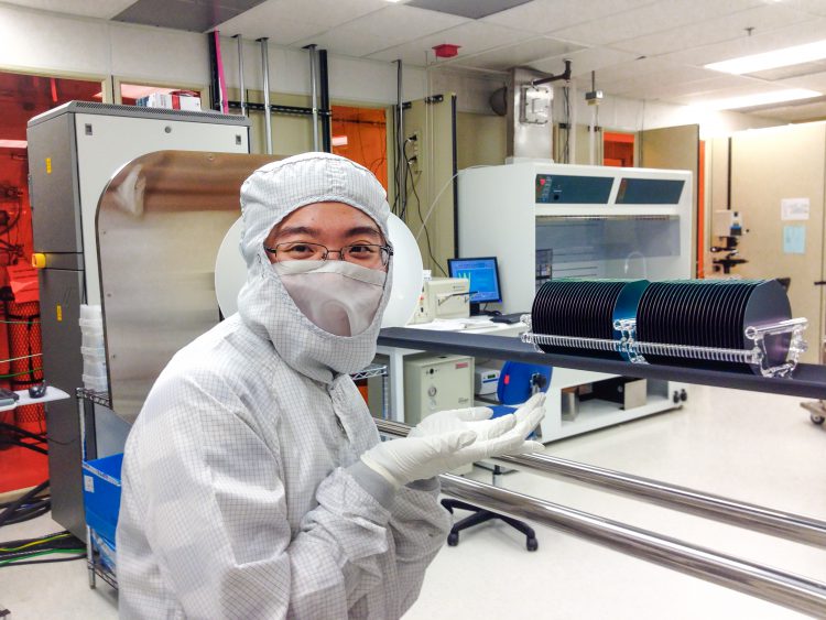
Zheyi Han in the WNF cleanroom.
Q: Tell us about your research.
A: For my doctoral thesis with ECE Professor Karl Böhringer, I have been working on the development of a compact optical system with adjustable focus that could be used in cell phones, entertainment (i.e. mixed reality displays), robotics, aerospace and biomedical systems (i.e. endoscopes). To create such a compact optical system, I integrated 2D optical elements, known as metasurfaces, into a micro-electromechanical system (MEMS)-driven Alvarez structure. In this structure, the focal length is determined by the overlapping area between two metasurfaces. MEMS actuators move the metasurfaces laterally to change the extent to which the metasurfaces overlap and in turn adjust the focal length. A relatively small movement is needed to change the focal length, making this system very compact. Moreover, compared to the tunable lenses that have previously been reported, this system consumses less power, focuses quicker, is less expensive and has the potential to be scalably produced.
Q: How has the WNF helped you to carry out your research?
A: We fabricate all of our MEMS metalens prototypes at the WNF. The convenient, on-campus location means that I can work in the facility myself which has allowed me to gain a much deeper understanding of the tools and processes involved in nanofabrication. It also means that I am able to experiement and iterate in a timely manner – something that would be far more difficult and time-consuming if we had to send our materials to another facility. In my time at WNF, I’ve found the WNF staff engineers to be a great resource. They are extremely knowledgable both as a result of their past experience and training, but also as a result of working with so many users who are doing different things. They have a great sense for what works and what doesn’t work when it comes to designing a successful process. Their suggestions and feedback have been super valuable when I’ve developed new processes.
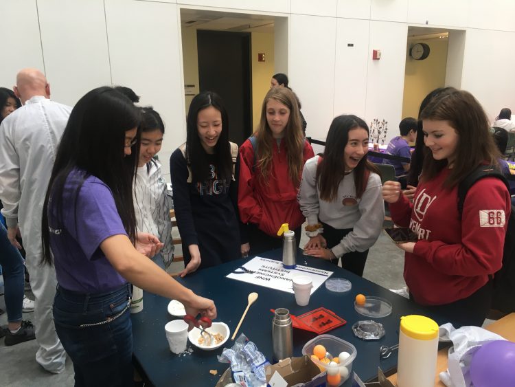
Han facilitates an interactive activity at the 2019 College of Engineering Discovery Days.
Q: You frequently volunteer for community education and outreach activities with UW. Why do you think STEM outreach is so important?
A: If you look at the world around us, almost everything is shaped by advances in science and technology. Through education and outreach, we as scientists and engineers can help all members of society, young and old, appreciate the great power of science and technology, while also emphasizing the importance of carefully considering how these technologies will be used.
Because the general public is not super familiar with nanotechnology, events like Nano Days at the Pacific Science Center and Engineering Discovery Days on the UW campus are great opportunities to help the public understand what nanotechnology is and how it can be used as a powerful tool to solve problems.
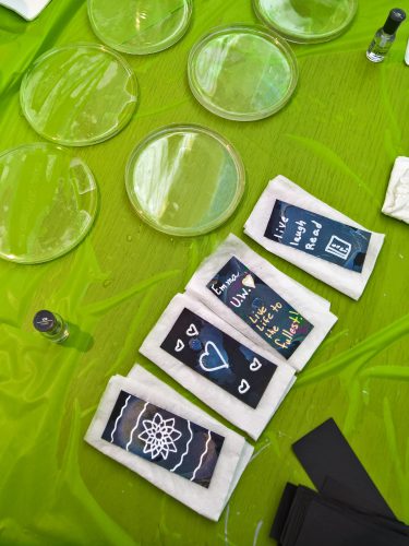
As part of a Nano Days at the Pacific Science Center, Han used clear nailpolish to demonstrate how the structure of a material at the nanoscale can impact its behavior at the macroscale. Find this activity on the NISE website: Exploring Materials – Thin Films.
As an added benefit, teaching and outreach activities provide new forums for me to practice my technical communication skills with broader audiences that include individuals that may or may not have STEM backgrounds.
Q: You will be graduating this fall. What’s next for you?
A: Last summer I interned at Google where I worked with a hardware team supporting Google’s technology infrastructure (e.g. data centers). While not an externally facing product, this infrastructure is critical to Google’s business. I had never worked in industry before, so this experience opened my eyes to what it is like to be an industrial researcher and I really enjoyed it. After graduation, I hope to join an industrial research lab focused on the design and development of transducer devices for a wide range of commercial applications.
And hopefully, I will still have some spare time to volunteer at STEM education and outreach activities!